
Every age in the history of human civilisation has a signature material, from the Stone Age, to the Bronze and Iron Ages. We might even call today’s information-driven society the Silicon Age.
Since the 1960s, silicon nanostructures, the building-blocks of microchips, have supercharged the development of electronics, communications, manufacturing, medicine, and more.
How small are these nanostructures? Very, very small – you could fit at least 3,000 silicon transistors onto the tip of a human hair. But there is a limit: below about 5 nanometres (5 millionths of a millimetre), it is hard to improve the performance of silicon devices any further.
So if we are about to exhaust the potential of silicon nanomaterials, what will be our next signature material? That’s where “atomaterials” come in.
What are atomaterials?
“Atomaterials” is short for “atomic materials”, so called because their properties depend on the precise configuration of their atoms. It is a new but rapidly developing field.
One example is graphene, which is made of carbon atoms. Unlike diamond, in which the carbon atoms form a rigid three-dimensional structure, graphene is made of single layer of carbon atoms, bonded together in a two-dimensional honeycomb lattice.
Diamond’s rigid structure is the reason for its celebrated hardness and longevity, making it the perfect material for high-end drill bits and expensive jewellery. In contrast, the two-dimensional form of carbon atoms in graphene allows electron travelling frictionless at a high speed giving ultrahigh conductivity and the outstanding in plane mechanical strength. Thus, graphene has broad applications in medicines, electronics, energy storage, light processing, and water filtration.
Using lasers, we can fashion these atomic structures into miniaturised devices with exceptional performance.
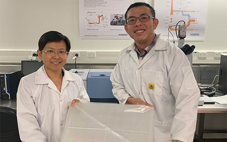
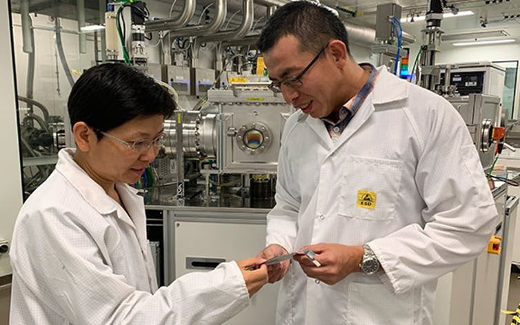
Using atomaterials, our lab has been working on a range of innovations, at various stages of development. They include:
- A magic cooling film. This film can cool the environment by up to 10℃ without using any electricity. By integrating such a film into a building, the electricity used for air conditioning can be reduced by 35%, and summer electricity blackouts effectively stopped. This will not only save electricity bills but also reduce greenhouse emissions.
- Heat-absorbing film. Some 97% of Earth’s water is in the oceans, and is salty and unusable without expensive processing. Efficiently removing salt from seawater could be a long-term solution to the growing global freshwater scarcity. With a solar-powered graphene film, this process can be made very efficient.
The film absorbs almost all the sunlight shining on it and converts it into heat. The temperature can be increased to 160℃ within 30 seconds. This heat can then distil seawater with an efficiency greater than 95%, and the distilled water is cleaner than tapwater. This low-cost technology can be suitable for domestic and industry applications.
- Smart sensing film. These flexible atomaterial films can incorporate a wide range of functions including environmental sensing, communication, and energy storage. They have a broad range of applications in healthcare, sports, advanced manufacturing, farming, and others. For example, smart films could monitor soil humidity near plants’ roots, thus helping to make agriculture more water-efficient.
- Ultrathin, ultra-lightweight lenses. The bulkiest part of a mobile phone camera is the lens, because it needs to be made of thick glass with particular optical properties. But lenses made with graphene can be mere millionths of a millimetre thick, and still deliver superb image quality. Such lenses could greatly reduce the weight and cost of everything from phones to space satellites.
- Near-instant power supply. We have developed an environmentally friendly supercapacitor from graphene that charges devices in seconds, and has a lifetime of millions of charge cycles. By attaching it to the back of a solar cell, it can store and deliver solar-generated energy whenever and wherever required. You will be free and truly mobile.
Where to next?
It can take years for some of these laboratory technologies to reach fruition. To try and speed up the process, we established the CTAM Global OpenLab to engage with industry, academia, government and the wider community and to promote sharing and collaboration. The lab was launched earlier this month at the International Conference on Nanomaterial and Atomaterial Sciences and Applications (ICNASA2020).
The world is facing pressing challenges, from climate change, to energy and resource scarcity, to our health and well-being.
Material innovation is more vital than ever and needs to be more efficient, design-driven and environmentally friendly. But these challenges can only be solved by joint effort from worldwide researchers, enterprise, industry and government with a sharing and open mindset.
- is Professor, Swinburne University of Technology
- This article first appeared on The Conversation

